Europe’s Semiconductor Strategy Is Quietly Changing
Why Chips Act 2.0 increasingly reflects a broader shift from technological sovereignty toward strategic indispensability inside the global AI economy
For years, Europe’s semiconductor ambitions largely focused on rebuilding manufacturing capacity and reducing dependence on foreign supply chains. But as AI infrastructure rapidly transforms the global technology landscape, Europe is beginning to rethink what technological power actually means.
When the European Union launched the original Chips Act in 2022, the political objective appeared relatively straightforward.
Europe wanted to reduce its dependence on Asian semiconductor manufacturing, strengthen domestic industrial resilience and regain a stronger position inside the global chip economy after pandemic-era shortages exposed the fragility of supply chains.
At the time, the strategy largely revolved around fabs.
Large-scale manufacturing plants became symbolic of technological sovereignty itself. Semiconductor power was still primarily understood through the lens of production volume, node size and industrial scale. But over the past two years, the global semiconductor landscape has changed dramatically.
Artificial intelligence systems are rapidly increasing the importance of advanced packaging, heterogeneous integration and hyperscale compute infrastructure. Increasingly, the challenge is no longer simply producing advanced chips — but physically integrating them into functioning AI architectures.
That shift is forcing Europe to reconsider its semiconductor strategy at a much deeper level.
The rise of the invisible infrastructure layer
One of the most important transformations inside the semiconductor industry is occurring far away from the public spotlight.
Modern AI systems increasingly depend on advanced packaging technologies capable of connecting multiple chiplets, memory systems and interconnect layers into one unified computational environment.
In practice, packaging is becoming computational architecture itself. This represents a major departure from earlier semiconductor eras. For decades, the industry focused primarily on shrinking transistors and improving front-end manufacturing efficiency. But physical, thermal and energy constraints are now limiting how far traditional monolithic chip scaling can continue.
As a result, the industry is shifting toward modular architectures built around heterogeneous integration.
That dramatically increases the importance of the back-end of semiconductor production — particularly OSAT (Outsourced Semiconductor Assembly and Test) and advanced packaging infrastructure. And this is precisely where Europe discovered a strategic vulnerability.
Even if Europe successfully expands domestic chip production, much of the integration layer transforming those chips into functioning AI systems still remains concentrated in Asia.
The semiconductor debate is therefore no longer simply about manufacturing chips. Increasingly, it is about controlling the infrastructure layers connecting entire computational ecosystems together.
Italy and the emergence of a European packaging corridor
This realization is quietly reshaping Europe’s industrial geography.
While semiconductor attention traditionally concentrated around northern European manufacturing and research ecosystems, Italy is increasingly emerging as one of the continent’s most strategically important locations for advanced packaging and systems integration.
The clearest example is Silicon Box in Novara.
The Singapore-based company is building one of Europe’s largest advanced packaging facilities, supported under the broader framework of the European Chips Act. The project focuses heavily on panel-level packaging and three-dimensional chip integration — technologies becoming increasingly essential for large-scale AI infrastructure.
Importantly, the European Commission granted the project Open EU Foundry (OEF) status, reflecting a broader institutional recognition that advanced packaging is no longer peripheral manufacturing infrastructure. It is strategic infrastructure.
At the same time, STMicroelectronics continues expanding its role inside Europe’s semiconductor ecosystem through major investments in Silicon Carbide technologies and power electronics in Catania, Sicily.
Together, these developments suggest something larger may be emerging:
a southern European semiconductor corridor focused less on manufacturing scale alone and more on systems integration, packaging and industrial coordination.
The AI back-end problem
This shift is also revealing one of the semiconductor industry’s fastest-growing bottlenecks.
AI infrastructure increasingly depends on highly specialized packaging platforms capable of integrating enormous computational density while managing heat, energy delivery and ultra-fast data transfer.
Companies such as Nvidia now rely heavily on advanced packaging systems like TSMC’s CoWoS technology to scale AI accelerators. In practice, some of the world’s most critical AI infrastructure layers remain concentrated around a relatively small number of facilities in Taiwan. This creates significant geopolitical exposure.
The bottleneck is no longer simply access to advanced chips themselves. Increasingly, it is access to the packaging ecosystems capable of integrating those chips into functioning AI systems.
That reality is gradually reshaping policy discussions surrounding Chips Act 2.0.
From sovereignty to indispensability
Perhaps the most important transformation unfolding inside Europe is philosophical.
The original Chips Act largely reflected the language of sovereignty and strategic autonomy. The assumption was that resilience required rebuilding domestic production capacity and reducing external dependence.
But the semiconductor industry may simply be too globally interconnected for full autonomy to remain realistic.
Instead, Europe increasingly appears to be pursuing something different:
technological indispensability.
Under this approach, Europe does not necessarily need to dominate every layer of the semiconductor supply chain. But it does need to control enough critical infrastructure layers that the global ecosystem cannot easily function without European participation.
This logic already applies to:
- ASML’s lithography systems,
- European industrial automation,
- photonics,
- automotive semiconductors,
- power electronics,
- and increasingly, advanced packaging itself.
In this emerging model, resilience comes less from isolation and more from structural embeddedness inside the global technology stack.
The implications extend far beyond semiconductors alone.
As AI infrastructure increasingly shapes energy systems, industrial productivity, military capability and digital governance, semiconductor ecosystems are evolving into foundational geopolitical infrastructure.
And Europe appears determined to ensure it remains part of that architecture.
Series — CHIPS ACT 2.0: The New European Semiconductor Architecture
This article is part of an Altair Media Europe series examining how Europe is redefining its semiconductor strategy in the age of AI infrastructure, geopolitical fragmentation and technological interdependence.
The series explores the growing importance of advanced packaging, OSAT, photonics, industrial ecosystems and systems integration as Europe gradually shifts from the pursuit of full technological autonomy toward a strategy of technological indispensability.
Part I — The Missing Layer
Why Europe’s semiconductor strategy is shifting from manufacturing scale to systems integration.
Part II — Italy and Europe’s Packaging Corridor
How Italy is positioning itself as a strategic hub for advanced packaging and semiconductor integration.
Part III — The AI Back-End Problem
Why advanced packaging is rapidly becoming one of the most critical bottlenecks in global AI infrastructure.
Part IV — From Sovereignty to Indispensability
How Chips Act 2.0 may signal a broader transformation in Europe’s technological and industrial thinking.
Link: https://altairmedia.eu/chips-act-2-0-the-new-european-semiconductor-architecture/
Credit
Artwork generated with AI for Altair Media Europe
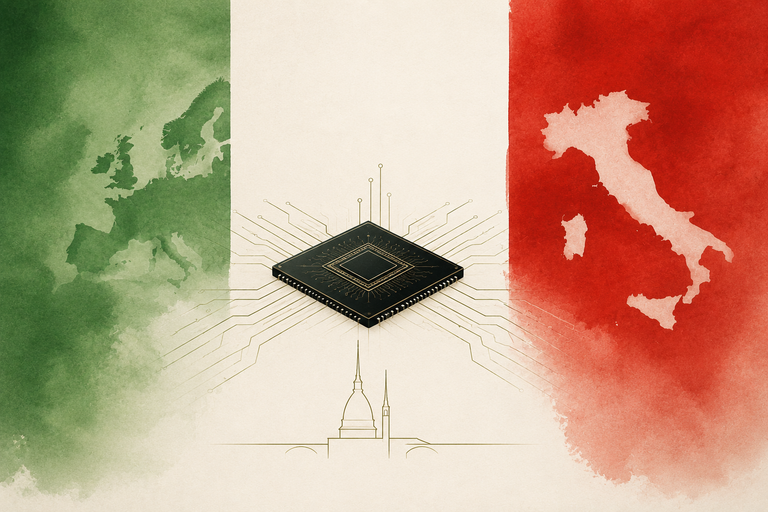
Caption
A minimalist illustration symbolizing Europe’s emerging semiconductor architecture. The image combines Italy, Europe and advanced chip infrastructure to reflect the continent’s growing focus on systems integration, AI infrastructure and technological indispensability in the age of Chips Act 2.0.