Posted by Altair Media on March 17, 2026 · Leave a Comment

At OFC 2026, one overlooked company reveals where power in the AI economy is shifting
The dominant narrative in artificial intelligence remains focused on compute. Faster GPUs, larger clusters, more advanced models. It is a story driven by scale and visibility—by the companies that design chips and train systems.
But as that scale increases, a different constraint is emerging. Less visible, less discussed, but increasingly decisive.
The bottleneck is no longer how much data can be processed. It is how that data moves.
At OFC 2026 in Los Angeles, this shift is difficult to ignore. The industry’s transition toward 1.6 terabit per second interconnects and the growing emphasis on extreme energy efficiency point to a deeper structural problem. Moving data between systems—quickly, reliably and without excessive power consumption—is becoming the limiting factor in AI deployment.
“Optics is no longer ‘behind the scenes’ — it is the connecting infrastructure that enables performance, efficiency and scalable growth in the AI-driven economy.”
Tetsuya Hayashi, General Chair OFC 2026 (Sumitomo Electric), OFC News Release 2026
Read More
Category: Analysis, Featured Headlines, Infrastructure, Technology · Tags: AIInfrastructure, Datacenters, DeepTech, DigitalEconomy, EuropeanTech, Photonics, Semiconductors, TechStrategy
Posted by Altair Media on March 12, 2026 · Leave a Comment

Why SCINTIL’s eLSFP Breakthrough Matters
The global race to scale artificial intelligence infrastructure is rapidly exposing the physical limits of data center connectivity. As AI clusters grow larger and faster, the amount of data that must move between processors, memory systems and racks is exploding. Traditional electrical interconnects—long the backbone of computing infrastructure—are struggling to keep up with the bandwidth, energy efficiency, and thermal constraints of modern AI systems.
Optical networking has emerged as the most promising solution to this bottleneck. By transmitting information through light rather than electricity, optical links can carry far more data with significantly lower power consumption over longer distances. Yet optical infrastructure itself is facing a new challenge: scaling efficiently to match the unprecedented demands of AI workloads.
A recent announcement by SCINTIL Photonics suggests that the next step in this evolution may already be underway. The company revealed its first DWDM eLSFP module, integrating eight lasers directly on a silicon photonics chip—a development that could significantly reshape how optical connectivity is designed for next-generation data centers.
“Today is a milestone I’ve been dreaming of since the beginning. Holding our first DWDM eLSFP module—a single chip with 8 lasers multiplexed on-chip—proves that heterogeneous InP/Silicon photonics can truly transform how the world connects with light.”
Sylvie Menezo
Founder & CEO, SCINTIL Photonics
Source: LinkedIn Corporate Update, March 2026
The announcement arrives just ahead of the industry’s most influential gathering for optical communications: the Optical Fiber Communication Conference, taking place March 15–19, 2026, at the Moscone Center in San Francisco. OFC is widely considered the global stage where the future of optical networking is unveiled and where large-scale partnerships between hyperscalers and photonics vendors are often formed.
The Technical Breakthrough
At the center of SCINTIL’s announcement is a new DWDM eLSFP optical module—a compact device that combines multiple advanced photonics technologies into a single integrated platform.
The acronym itself reveals the technological significance:
- DWDM (Dense Wavelength Division Multiplexing) enables multiple optical signals to travel simultaneously through a single fiber by using different wavelengths—or “colors”—of light.
- eLSFP (External Laser Source Form-factor Pluggable) refers to a new pluggable laser architecture in which the light source is separated from the optical engine that modulates the data.
The critical breakthrough lies in the level of integration achieved. SCINTIL’s chip contains eight lasers spaced at 100 or 200 GHz intervals, which are then multiplexed directly on the chip into a single optical output.
Traditionally, such architectures rely on multiple discrete lasers combined with external optical filters or multiplexers. Integrating these functions onto a single chip reduces the number of components required, simplifies packaging and improves overall efficiency.
Industry analysts estimate that on-chip DWDM integration can reduce optical packaging complexity by 40% to 60%, a major advantage for large-scale deployments where cost and reliability are paramount.
Why External Laser Sources Matter
One of the most important trends in modern optical networking is the shift toward external laser architectures.
In conventional optical transceivers, the laser source is located directly next to the photonic circuitry responsible for modulation and signal processing. While this design works for many applications, it becomes problematic in high-performance networking environments—especially inside AI infrastructure.
The reason is heat.
Switch ASICs and GPUs in AI clusters can generate enormous thermal loads. Placing delicate laser sources near these hot chips can degrade performance and shorten device lifetimes. External laser architectures solve this issue by physically separating the laser from the high-temperature computing components.
“The decoupling of the light source from the optical engine via the eLSFP standard is critical for the thermal management of next-generation 102.4T switches and AI clusters.”
Pascal Langlois
Co-Founder & Chairman, SCINTIL Photonics
Source: SCINTIL Technology Whitepaper / OFC Preview 2026
In this model, the laser sits in a cooler, serviceable pluggable module located at the front of a switch. Light is then delivered via fiber to the optical engines located near the processing silicon.
This approach not only improves thermal stability but also introduces operational flexibility. External laser modules can be replaced independently, allowing operators to service critical components without removing entire network switches.
Solving the Laser Integration Problem
Despite the promise of silicon photonics, one challenge has persisted for more than a decade: integrating efficient lasers directly onto silicon wafers.
Silicon itself cannot emit light efficiently. As a result, most photonic systems rely on external laser components made from Indium Phosphide (InP)—a compound semiconductor capable of generating coherent light.
SCINTIL’s technology addresses this limitation through heterogeneous integration, bonding InP laser structures directly onto silicon photonics wafers. This allows the lasers and photonic circuitry to be fabricated together as part of a unified chip.
“Integrating the laser source directly onto the Silicon Photonics wafer remains the ‘Holy Grail’ of the industry. SCINTIL’s ability to deliver an 8-channel DWDM source in a pluggable form factor addresses the urgent density requirements of AI-scale fabrics.”
Dr. Vladimir Kozlov
CEO & Founder, LightCounting
Source: LightCounting Market Report on Co-Packaged Optics & External Laser Sources
For years, silicon photonics manufacturers have relied on manual alignment or hybrid packaging techniques to attach laser sources to chips. These approaches increase cost and complexity, limiting the scalability of optical modules.
Direct integration could fundamentally change that equation.
The AI Data Center Connection
The urgency behind these innovations is largely driven by the rapid expansion of AI infrastructure.
Modern AI training clusters consist of thousands of GPUs connected through ultra-high-speed networks. As these clusters scale, the amount of data that must move between processors increases dramatically. Networking architectures are now evolving toward co-packaged optics (CPO) and optical switching fabrics designed specifically for AI workloads.
NVIDIA’s next-generation architectures and similar platforms from hyperscalers are expected to push network switches toward 102.4 terabit per second throughput and beyond. At these speeds, electrical signaling becomes increasingly inefficient, making optical interconnects essential.
However, optical systems must also evolve to meet new density and energy requirements.
Integrated multi-laser sources—such as the one demonstrated by SCINTIL—could enable more compact and efficient optical engines capable of supporting the enormous scale of AI clusters.
A Deep Technology Ecosystem
The announcement also reflects the strength of the European silicon photonics ecosystem.
SCINTIL operates as a fabless photonics startup, designing its technology while leveraging advanced semiconductor manufacturing partners. The company maintains deep ties to the photonics research community in Grenoble, one of Europe’s leading hubs for microelectronics and photonics innovation.
The reference in the announcement to “Frédéric” likely acknowledges the contributions of Frédéric Boeuf, a prominent silicon photonics expert previously associated with STMicroelectronics and the broader CEA-Leti ecosystem.
This ecosystem has played a critical role in advancing heterogeneous photonic integration, providing the scientific foundation for technologies that are now approaching commercial deployment.
The Strategic Implication
Taken together, SCINTIL’s demonstration signals a broader shift underway in the photonics industry.
For decades, optical networking systems were built from discrete optical components—individual lasers, modulators, filters, and detectors assembled through complex packaging processes.
Today, the industry is moving toward optical system-on-chip architectures, where these components are integrated directly onto semiconductor platforms.
In many ways, this transformation mirrors the history of electronic integrated circuits. Just as Moore’s Law drove the consolidation of electronic components into microchips, photonics is now undergoing a similar process of integration.
If scalable manufacturing follows, the result could be a dramatic reduction in the cost and energy consumption of optical interconnects—unlocking the next phase of growth for AI infrastructure.
The Road Ahead
While SCINTIL’s announcement represents an important milestone, the path to widespread adoption will depend on several factors.
The technology must demonstrate reliability at scale, compatibility with existing network architectures, and cost competitiveness against alternative solutions. Large-scale customer trials and design wins with networking vendors or hyperscalers will likely determine how quickly integrated laser modules move from demonstration to deployment.
OFC 2026 will therefore be an important test of industry momentum. With the world’s leading photonics companies, network equipment vendors, and hyperscalers gathering in San Francisco, the event will offer the first opportunity for the broader industry to evaluate the implications of this technology.
If the promise of integrated multi-laser silicon photonics holds, it could mark a turning point for optical networking—bringing the industry one step closer to fully integrated optical infrastructure designed for the AI era.
Photo credit
Illustration: AI-generated / OpenAI.
Caption
Conceptual illustration of a DWDM eLSFP optical module integrating multiple lasers on a silicon photonics chip for next-generation AI data center networks.
Category: Analysis, Featured, Infrastructure, Photonics · Tags: AI data centers, DWDM, external laser sources, hyperscale infrastructure, optical networking, photonic integration, semiconductor innovation, Silicon Photonics
Posted by Altair Media on March 7, 2026 · Leave a Comment
How Chips, Materials and Infrastructure Power the Intelligence Economy
Artificial intelligence is often described as a revolution in algorithms. The public conversation revolves around models, chatbots and software breakthroughs, while the race between technology companies is usually framed as a competition to build larger and more powerful AI systems.
Yet behind every AI model lies something far more complex: a vast industrial ecosystem spanning continents.
Modern AI hardware is not built in a single factory or even a single country. Instead, it is the product of a global relay race involving semiconductor design firms, specialized materials producers, lithography equipment manufacturers, advanced chip foundries and hyperscale data centers.
What appears to users as a digital technology is in reality the result of one of the most intricate supply chains ever constructed.
“The semiconductor supply chain is the most complex feat of human engineering in history. There is no such thing as a ‘local’ AI chip; every transistor relies on a global relay race.”
Jensen Huang
CEO & Founder, NVIDIA
Huang’s observation captures a fundamental truth about the AI economy. While artificial intelligence may operate in the digital realm, its foundation is profoundly physical. Every neural network ultimately depends on semiconductors manufactured through a planetary network of materials, machines and industrial processes.
Understanding the future of AI therefore requires understanding the global system that produces its hardware.
Silicon Valley: Where AI Chips Begin
The first step in the AI supply chain often begins in the United States, where semiconductor companies design the processors that power modern machine learning systems.
Companies such as NVIDIA, AMD and Apple create the architectures that define the performance of AI hardware. These chips contain tens of billions of transistors and are optimized to handle the parallel computations required for training neural networks.
Yet these companies rarely manufacture their own processors.
Instead, chip design firms rely on a distributed ecosystem of specialized suppliers and manufacturers across Asia, Europe and North America.
The journey of an AI processor has only just begun.
The Invisible Layer: Chemistry and Wafers
Before silicon chips can be manufactured, a range of highly specialized materials must be produced.
Silicon wafers—the circular substrates on which chips are fabricated—must be grown from ultra-pure crystals. These wafers are polished to atomic precision and prepared using a complex mix of chemicals and industrial gases.
One particularly critical ingredient is photoresist, a light-sensitive chemical used during lithography to pattern the microscopic circuits on a chip.
A handful of companies dominate this field, many of them based in Japan, including JSR Corporation and Shin‑Etsu Chemical.
The fragility of this layer of the supply chain is often underestimated. A disruption in the production of specialty chemicals or wafers can ripple through the global semiconductor industry for months.
In the AI era, even the chemistry of manufacturing has become strategically important.
The Dutch Bottleneck: Lithography
Once the materials are ready, the next step in the supply chain is lithography—the process of projecting microscopic patterns onto silicon wafers to create transistors.
This stage of the industry is dominated by a single company: ASML.
ASML builds the extreme ultraviolet (EUV) lithography machines used to manufacture the world’s most advanced semiconductors. These machines are among the most complex industrial systems ever produced, incorporating more than 100,000 components and requiring an international network of suppliers.
“We are not just selling machines; we are selling the ability for the world to continue its digital evolution. Without the collective ecosystem of thousands of suppliers, EUV simply wouldn’t exist.”
Christophe Fouquet
CEO, ASML
Lithography equipment from ASML enables semiconductor manufacturers to create chips with features measured in nanometers—smaller than a virus particle.
Without these machines, the high-performance processors required for artificial intelligence would simply not exist.
Taiwan: The Manufacturing Core
After design and lithography, the next stage of the supply chain takes place in semiconductor foundries.
The most important of these is TSMC, the Taiwanese company that manufactures the majority of the world’s most advanced chips.
TSMC produces processors for companies including NVIDIA, AMD and Apple, making Taiwan one of the most critical nodes in the global technology economy.
This concentration of advanced manufacturing has created what some analysts call the “silicon shield”—the idea that Taiwan’s central role in semiconductor production makes it strategically important to the entire global economy.
“Silicon Shield is a real concept. The world’s reliance on advanced logic chips produced in Hsinchu is both the greatest guarantor of stability and our greatest vulnerability.”
Morris Chang
Founder, TSMC
The geopolitical implications of this concentration are profound. Any disruption to semiconductor manufacturing in Taiwan would have immediate consequences for industries ranging from smartphones to artificial intelligence.
The Hidden Bottleneck: Advanced Packaging
Once chips are fabricated, they must be assembled into functional systems.
This process—known as advanced packaging—has become one of the most critical steps in the AI supply chain.
Modern AI processors are no longer single pieces of silicon. Instead, they combine multiple chiplets, high-bandwidth memory modules and specialized interconnect technologies.
One of the most important packaging techniques used for AI chips is CoWoS (Chip on Wafer on Substrate), a technology developed by TSMC that allows multiple components to be integrated into a single high-performance package.
The rapid growth of AI has created an unexpected bottleneck in this stage of production. Demand for advanced packaging capacity—particularly for NVIDIA’s GPUs—has outpaced supply, turning packaging into one of the most critical constraints in AI hardware manufacturing.
In many ways, the race for better packaging has become a new frontier in semiconductor innovation.
Data Centers: Where the Supply Chain Converges
The final destination of AI hardware is the data center.
Hyperscale cloud providers such as Microsoft, Amazon, Google and Meta operate massive facilities filled with thousands of GPUs designed to train and run AI models.
These data centers combine all the elements of the AI supply chain:
• advanced semiconductor chips
• high-speed networking infrastructure
• optical interconnects
• cooling systems
• enormous electricity supplies
The scale of these facilities is unprecedented.
“The bottleneck for AI is no longer just the code or the data. It is the physics of the grid. We are building the cathedrals of the 21st century and they require more power than mid-sized cities.”
Satya Nadella
CEO, Microsoft
Nadella’s comparison of data centers to cathedrals reflects the industrial scale of modern AI infrastructure. These facilities represent a new form of digital architecture, designed to transform electricity and hardware into machine intelligence.
Hardware Constraining the World
For much of the past two decades, the dominant narrative in technology was that software was transforming every industry.
Today, the pendulum is beginning to swing back toward hardware.
The rapid expansion of artificial intelligence has exposed the physical constraints of computing: semiconductor manufacturing capacity, materials supply chains, energy infrastructure and geopolitical stability.
“AI is often discussed as a disembodied intelligence, but its soul is made of silicon, copper and neon. We are moving from the era of ‘software is eating the world’ to ‘hardware is constraining the world.’”
Pat Gelsinger
CEO, Intel
Gelsinger’s remark captures the new reality of the AI era. As machine intelligence scales, the physical infrastructure that supports it becomes increasingly important.
The limits of artificial intelligence are no longer purely computational.
They are industrial.
The Planetary Infrastructure of Intelligence
Seen from a distance, the AI supply chain resembles a global technological ecosystem.
Chip designs originate in Silicon Valley.
Lithography machines are built in the Netherlands.
Manufacturing takes place in Taiwan and South Korea.
Advanced packaging is concentrated across Asia.
And the resulting processors are deployed in data centers around the world.
Together, these systems form a planetary network of infrastructure designed to produce intelligence at scale.
Artificial intelligence may appear intangible, but it rests on one of the most complex industrial systems humanity has ever created.
In the end, the AI revolution is not just a story about algorithms. It is a story about the global machinery that makes those algorithms possible.
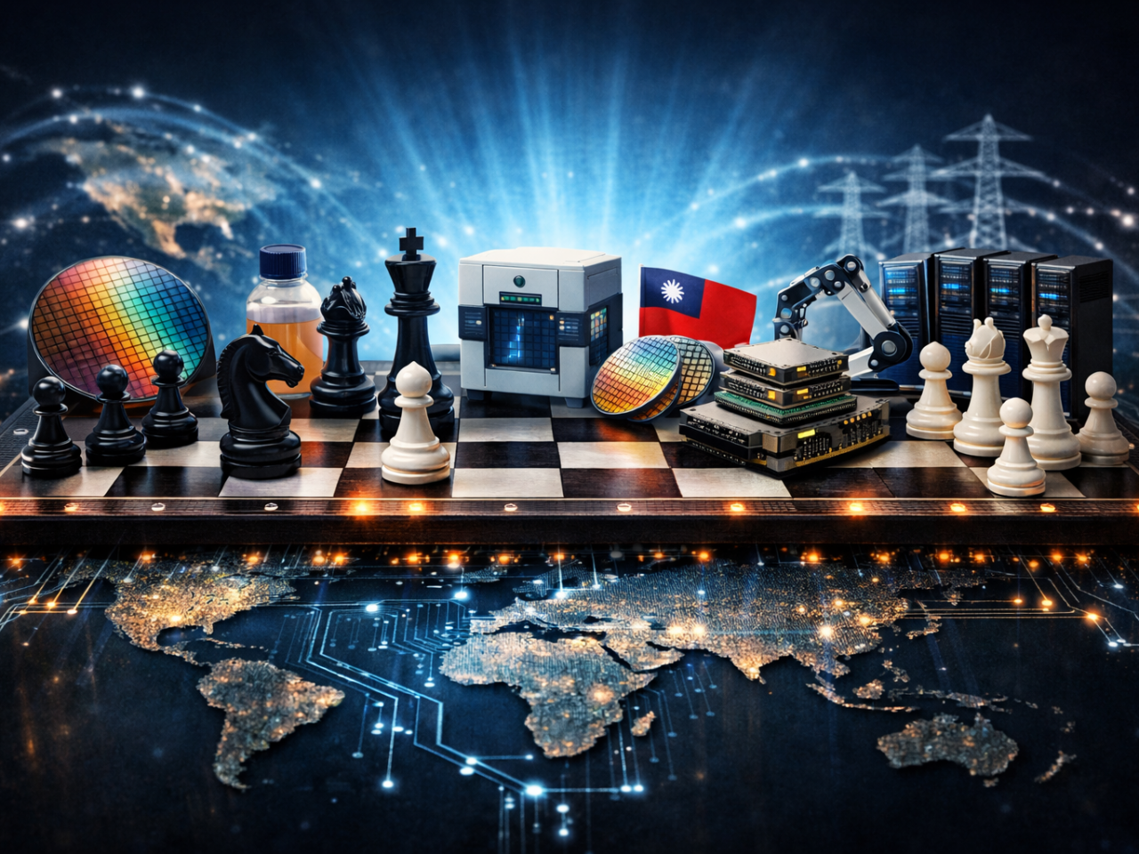
Photo credit
AI-generated illustration / OpenAI
Caption
Conceptual illustration of the global AI supply chain as a strategic chessboard, where semiconductor design, lithography, manufacturing and data center infrastructure interact across continents to power the emerging intelligence economy.
Artificial intelligence is not just about software and algorithms. It also depends on a vast physical infrastructure of chips, photonics and data centers.
Explore the series: https://altairmedia.us/the-ai-infrastructure-stack/
Category: Analysis, Featured, Industry, Semiconductors, Supply Chains · Tags: AI Hardware, AI supply chain, chip manufacturing, data centers, geopolitics of technology, global technology infrastructure, semiconductor ecosystem, Semiconductors
Posted by Altair Media on March 6, 2026 · Leave a Comment

Why Power May Become the Real Bottleneck of Artificial Intelligence
Artificial intelligence is often described as a revolution in software. Advances in machine learning models, neural networks and algorithms dominate headlines, while the race between technology giants focuses largely on who can build the most powerful chips.
But behind the software layer lies a far more physical reality. Modern AI systems depend on vast networks of processors running inside hyperscale data centers—facilities that resemble industrial infrastructure more than traditional computing environments.
As artificial intelligence scales, these facilities are consuming extraordinary amounts of electricity. The challenge facing the industry is no longer simply how to design faster chips or train larger models. Increasingly, it is about how to supply enough power to run them.
In other words, the next bottleneck in the AI revolution may not be compute or networking.
It may simply be energy.
“The biggest issue we are now having is not a compute glut, but power. I have a bunch of chips sitting in inventory that I can’t plug in because I don’t have the ‘warm shells’ to put them in.”
Satya Nadella
CEO, Microsoft
Statement referenced in industry discussions, 2025
Nadella’s observation highlights a paradox of the current AI boom. Technology companies are producing increasingly powerful processors and building enormous clusters of GPUs, yet many of those systems cannot be fully deployed because the infrastructure supplying them with electricity has not kept pace.
The AI race is therefore evolving into something broader than a competition in algorithms or hardware.
It is becoming a competition in energy.
The Rise of the AI Data Center
The modern AI data center bears little resemblance to the cloud infrastructure of a decade ago.
Where earlier facilities focused primarily on storing data and running web services, AI data centers function more like computational factories. They host thousands—sometimes tens of thousands—of specialized processors designed to train and operate large language models and other machine learning systems.
These clusters rely on GPUs from companies such as NVIDIA and AMD, connected through high-speed networking and supported by advanced cooling systems.
The scale is staggering.
A single large AI cluster can consume hundreds of megawatts of electricity—comparable to the power requirements of a small city. Hyperscale operators such as Amazon, Google and Microsoft are now planning data center campuses that require gigawatts of power capacity.
This shift is transforming how infrastructure is designed. Instead of simply building server farms near network hubs, companies must increasingly locate new data centers near reliable energy sources and transmission infrastructure.
In many regions, electricity availability has become the primary constraint.
GPUs and the Power Curve
The rapid rise in energy demand is closely tied to the evolution of AI hardware.
Each new generation of AI processors delivers dramatically higher computational performance. Advanced architectures incorporate massive parallel processing, high-bandwidth memory and increasingly sophisticated interconnect technologies.
But these improvements also increase energy consumption.
Training state-of-the-art AI models requires thousands of GPUs operating simultaneously, often for weeks or months at a time. Running those systems generates enormous electrical loads and produces large amounts of heat, which must then be removed through equally energy-intensive cooling systems.
Even the companies designing these processors recognize the magnitude of the challenge.
“The next industrial revolution will require an extraordinary amount of energy. Datacenters are no longer just places to store data; they are AI factories.”
Jensen Huang
CEO, NVIDIA
Huang’s description of data centers as “AI factories” reflects a broader shift in how computing infrastructure is perceived. Instead of passive repositories of information, these facilities are increasingly viewed as industrial systems that transform electricity into intelligence.
Like traditional factories, they require a constant and reliable supply of energy to operate.
The Grid Problem
The growing energy demand of AI is beginning to expose limitations in existing electrical infrastructure.
In many parts of the world, electricity grids were not designed to support large concentrations of energy-intensive computing facilities. Transmission lines, substations and transformers often lack the capacity to deliver the power required by new AI data centers.
As a result, utilities and regulators in several regions are reporting long waiting lists for new grid connections.
Developers planning large data centers must sometimes wait years for the necessary infrastructure upgrades. In other cases, projects are being relocated entirely to areas with more abundant energy supplies.
This emerging constraint has led some industry leaders to warn that electricity itself may become the next major shortage in the technology sector.
“The chip shortage may be behind us, but the next shortage will be electricity and transformers.”
Elon Musk
CEO, Tesla and xAI
The observation captures the essence of the challenge: even if the semiconductor industry can produce enough processors, those processors still need power to operate.
And the energy infrastructure required to support them cannot be built overnight.
The Return of Nuclear
Faced with rising energy demand, several technology companies are exploring new approaches to securing reliable power.
Among the most notable trends is a renewed interest in nuclear energy.
Unlike solar or wind power, nuclear reactors provide continuous baseload electricity, making them particularly attractive for facilities that must operate around the clock. They also produce minimal carbon emissions, an important factor for companies with ambitious climate commitments.
In recent years, major technology firms have begun investing in nuclear energy projects and signing long-term agreements with energy providers.
“We need to move toward nuclear, wind and solar very quickly to meet this demand without destroying the climate.”
Sam Altman
CEO, OpenAI
One emerging technology attracting attention is the Small Modular Reactor (SMR), a new generation of compact nuclear reactors designed to be easier and faster to deploy than traditional plants.
If widely adopted, SMRs could provide dedicated power sources for future data center campuses, effectively turning energy generation into an integral part of digital infrastructure.
In that sense, the growth of artificial intelligence could inadvertently accelerate the development of next-generation nuclear technologies.
Efficiency: The Race to Reduce Energy per AI Operation
While expanding energy supply is one solution, the industry is also pursuing another strategy: improving efficiency.
Reducing the amount of energy required for each AI computation could dramatically lower the total power consumption of large-scale systems.
Researchers and engineers are exploring several approaches to achieve this goal.
Specialized AI accelerators are designed to perform machine learning tasks more efficiently than general-purpose processors. Advances in semiconductor design aim to reduce energy consumption per transistor operation. Meanwhile, new networking technologies—such as optical interconnects based on silicon photonics—promise to reduce the energy required to move data between processors.
These developments connect directly to earlier layers of the AI infrastructure stack.
Faster photonic interconnects can move data more efficiently than traditional electrical connections, while new chip architectures can perform complex computations using less power.
Each incremental improvement helps reduce the energy footprint of AI systems.
But the scale of demand continues to grow.
Energy, Compute and the Physics of Intelligence
At its core, artificial intelligence is not merely a software phenomenon.
It is a physical process.
Every calculation performed by a neural network consumes energy. Every data transfer between processors requires electricity. Every data center must dissipate heat generated by billions of electronic operations per second.
This reality has led some researchers to describe AI development as a confrontation with the fundamental limits of physics.
“The only thing blocking real-time reasoning at scale is inference cost. Ultimately we are fighting the physics of energy per operation.”
Dario Amodei
CEO, Anthropic
Seen from this perspective, the evolution of artificial intelligence is inseparable from advances in energy systems, semiconductor technology and physical infrastructure.
Scaling intelligence requires scaling the energy systems that sustain it.
The Power Behind the AI Era
The AI revolution is often framed as a race between algorithms, datasets and chip manufacturers.
Yet the deeper story may be more fundamental.
Behind every AI model lies a vast network of infrastructure: semiconductor fabrication plants, optical networks, cooling systems, transmission lines and power stations. Together, these systems convert electricity into computation and computation into intelligence.
As AI continues to expand, the defining constraint may not be the availability of processors or the sophistication of algorithms.
It may simply be whether the world can produce—and deliver—enough electricity to power them.
In that sense, the future of artificial intelligence may depend as much on energy infrastructure as it does on machine learning breakthroughs.
The AI revolution, it turns out, runs on power.
Artificial intelligence is not just about software and algorithms. It also depends on a vast physical infrastructure of chips, photonics and data centers.
Explore the series: https://altairmedia.us/the-ai-infrastructure-stack/
Photo credit
AI illustration / OpenAI
Caption
Artificial intelligence is increasingly limited not only by chips and networks, but by the energy required to power large-scale computing infrastructure.
This shift—from electrons to photons—is part of a deeper transformation in how we understand intelligence: not just as software, but as something rooted in physics, energy and infrastructure.
I explore this idea further in my ebook The Age of Light — Meaning, Machines and the Physics of Intelligence, about how photonics and physical computing architectures are reshaping AI and global power.
Available worldwide on Amazon (Kindle):
https://www.amazon.com/dp/B0GMXLX56T
Posted by Altair Media on March 6, 2026 · Leave a Comment

How Dutch Photonics Could Shape the Future of AI Infrastructure
The global race to build artificial intelligence is often framed as a contest between American technology giants and Asian chip manufacturers. Silicon Valley dominates the headlines with massive investments in AI chips and data centers, while Taiwan and South Korea supply the manufacturing muscle that turns designs into silicon.
Yet behind this visible competition lies a quieter infrastructure race—one that determines how quickly data can move between the processors that power modern AI systems.
As AI models grow larger and more complex, the real bottleneck is shifting. The challenge is no longer simply building faster processors. It is ensuring that thousands of processors inside hyperscale data centers can exchange data quickly enough to function as a single machine.
Some of the key technologies addressing that challenge—especially those involving photonics and optical communication—have roots in a place that rarely appears in discussions about the AI race: the Dutch city of Eindhoven.
“The real breakthrough is not the laser alone, but the integration. We are moving from a world where we glue components together to a world where complete optical systems can be printed on a millimeter scale. The Netherlands holds the blueprint for this transition.”
Prof. Dr. Martijn Heck
Professor of Photonic Integration, Eindhoven University of Technology
For decades, researchers at the Eindhoven University of Technology—often referred to as TU/e—have been working on technologies that guide light through microscopic circuits on a chip. Known as integrated photonics, these systems promise to transmit data using photons instead of electrons, dramatically increasing bandwidth while reducing energy consumption.
That work is now becoming central to the infrastructure behind artificial intelligence.
From Compute Power to Data Movement
The first phase of the AI boom focused on raw computational power. Companies such as NVIDIA and AMD built specialized processors capable of training massive machine learning models. Hyperscale cloud providers—including Microsoft, Meta and Amazon—then assembled thousands of those chips into enormous AI clusters.
But scaling these systems revealed a new constraint. The processors must constantly exchange model parameters, training data and intermediate results. As clusters grow to tens of thousands of chips, the amount of data flowing between them becomes staggering.
Electrical interconnects based on copper cables struggle at these speeds. They consume increasing amounts of power and generate heat, making them inefficient for the massive scale of modern AI infrastructure.
This is why engineers are increasingly turning to photonics.
Instead of transmitting electrical signals, photonic systems move data using light traveling through optical waveguides. The approach offers higher bandwidth, lower energy consumption and significantly less heat generation—key advantages in massive data centers where power efficiency is critical.
Companies such as OpenLight in the United States are now pushing these technologies toward large-scale deployment, integrating lasers directly onto silicon photonics chips designed for high-speed data center networking.
Yet the intellectual foundations for many of these developments trace back to research ecosystems such as the one in Eindhoven.
Silicon and Indium Phosphide: Two Worlds Converging
One of the central technical challenges in photonics is the laser.
Silicon—the material used to manufacture most modern chips—is excellent for electronics but poor at generating light. Optical systems therefore require another material capable of efficiently producing laser signals.
That material is often Indium Phosphide, a compound semiconductor widely used in high-performance photonic devices.
Eindhoven’s photonics ecosystem has become one of the world’s leading centers of expertise in indium phosphide technology. Researchers and startups in the region have spent decades refining methods to integrate photonic components into compact, scalable systems.
The emerging solution for AI infrastructure may be a hybrid architecture that combines both materials: silicon for electronic circuitry and indium phosphide for laser generation.
“Silicon is an excellent material for electronics, but it does not naturally emit light. For that you need indium phosphide. The future of AI infrastructure will likely depend on hybrid platforms that combine the strengths of both.”
Prof. Dr. Martijn Heck
Photonic Integration Researcher, TU Eindhoven (interpretation of his published research perspectives)
This hybrid approach is precisely what many companies developing next-generation photonics platforms are pursuing today.
Brainport: Europe’s Photonics Ecosystem
The Eindhoven region—often referred to as Brainport—has evolved into one of Europe’s most concentrated clusters for high-tech innovation.
The ecosystem includes not only the university but also research institutes, startups and specialized manufacturing companies focused on photonic technologies.
One of the most notable is SMART Photonics, a semiconductor foundry dedicated to producing photonic integrated circuits. Unlike traditional semiconductor fabs that manufacture digital processors, SMART Photonics focuses on optical chips capable of guiding and manipulating light.
“We are on the verge of a massive rollout. Demand from the AI market for faster and more energy-efficient connections is the catalyst that is pushing photonic chips out of the lab and directly into the backbone of the internet.”
Luc Augustin
Chief Technology Officer, SMART Photonics
This shift reflects the growing realization that optical technologies are not just useful for telecommunications networks spanning continents. They are becoming essential inside the data centers that power cloud computing and artificial intelligence.
Supporting this ecosystem is PhotonDelta, a national initiative designed to strengthen the Netherlands’ position in integrated photonics. The program aims to build a complete value chain—from academic research to industrial manufacturing—capable of competing globally.
The Role of ASML
Any discussion of the Dutch semiconductor ecosystem inevitably leads to ASML, the world’s only manufacturer of extreme ultraviolet (EUV) lithography machines.
These machines are essential for producing the most advanced semiconductor chips and are used by manufacturers such as TSMC, Intel and Samsung Electronics.
While ASML is primarily associated with digital semiconductor manufacturing, the broader Brainport ecosystem it anchors is increasingly relevant to photonics as well. The same precision engineering, advanced materials science and specialized supply chains that enabled EUV lithography are helping drive innovation in photonic technologies.
In that sense, the Dutch semiconductor ecosystem is expanding from enabling the world’s fastest processors to influencing the technologies that allow those processors to communicate.
Photonic Sovereignty
For Europe, photonics represents more than just a technological opportunity. It may also offer a strategic position in the global technology landscape.
While the United States dominates AI software and chip design and Asia leads in semiconductor manufacturing, Europe has developed significant expertise in photonic hardware and optical systems.
“Photonics is an opportunity for Europe not just to consume technology, but to become an architect of the infrastructure on which the global AI ecosystem will run.”
Eelko Brinkhoff
CEO, PhotonDelta
If optical interconnects become as critical to AI systems as GPUs themselves, regions with strong photonics ecosystems could play a disproportionately important role in shaping the next generation of computing infrastructure.
The Quiet Backbone of the AI Era
The rapid rise of artificial intelligence has captured global attention. Governments are investing billions in semiconductor manufacturing, cloud infrastructure and AI research.
Yet the future of AI may depend on technologies that receive far less attention.
The processors inside AI systems may be the engines of the digital age, but engines alone do not build highways. Without the infrastructure that allows those processors to exchange data at extraordinary speeds, even the most powerful chips would be constrained by network bottlenecks.
In that sense, the AI revolution is not only about faster chips.
It is also about the optical pathways that connect them—and those pathways may lead, unexpectedly, through Eindhoven.
Photo credit
AI-generated illustration / OpenAI
Caption
Conceptual illustration of integrated photonics chips transmitting data with light. Optical interconnects are emerging as a critical technology for connecting AI processors in hyperscale data centers.
This shift—from electrons to photons—is part of a deeper transformation in how we understand intelligence: not just as software, but as something rooted in physics, energy and infrastructure.
I explore this idea further in my ebook The Age of Light — Meaning, Machines and the Physics of Intelligence, about how photonics and physical computing architectures are reshaping AI and global power.
Available worldwide on Amazon (Kindle):
https://www.amazon.com/dp/B0GMXLX56T
Category: Analysis, Featured, Industry, Photonics · Tags: AI infrastructure, ASML, data center technology, Eindhoven photonics ecosystem, integrated photonics, optical networking, Semiconductors, Silicon Photonics